

 Time-Dependent Density-Functional Theory: Concepts and Applications
Cite
Appendix K
Semiconductor quantum wells are an important class of nanostructures, with many technological applications in optoelectronics and elsewhere. Our particular interest in quantum wells is not so much because of all these wonderful device applications, but because they represent very simple, quasi-one-dimensional model systems which are nice for benchmark calculations in TDDFT. In this appendix, we will review the basic concepts of the electronic structure and excitations of quantum wells, focusing on a particular type of excitation called intersubband plasmon. Readers who wish for a more in-depth treatment of semiconductor nanostructures can choose among a large number of texts; a good place to start is the books by Davies (1998) and Harrison (2005).
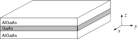
The basic geometry of a quantum well is illustrated in Fig. K.1: a layer of semiconductor material A, typically only a few tens of nanometers thick, is sandwiched between layers of another material B. The combination GaAs/AlxGa1–xAs, with 0 < x < 0.3, is very popular since the two materials are almost perfectly lattice-matched. Here and in the following, we take the z-axis to be perpendicular to the layers, i.e., along the direction in which the heterostructure has been grown. The system is assumed to be infinitely extended in the x–y plane. In practice, the system B–A–B of Fig. K.1 will be grown on a substrate and surrounded by additional spacer layers, which, however, are not important for the following considerations.
Basic geometry of a GaAs/AlGaAs quantum well.
We will consider quantum well systems that are n-doped; the doping centers are sufficiently far away (this is called “remote doping” or “modulation doping”) that the ionized impurities have little influence on the electron dynamics in the well. The electrons from these remote doping centers accumulate in the quantum well, and the electronic sheet density N s (which measures the number of electrons per unit area) is assumed to be given. In the following, we will describe how to calculate the electronic ground state and dynamics using (TD)DFT in the effective-mass approximation.
K.1 Effective-mass approximation and subband levels
The electronic structure in a periodic solid reflects the basic symmetries of the under-lying crystal lattice. According to Bloch's theorem, the electronic states in the periodic potential have the form of modulated plane waves, ψ nq(r) = u nq(r)e iqr, where u nq is a lattice-periodic function, with band index n and wave vector q (disregarding spin for now). The associated single-particle energies ε nq can be computed using standard band structure techniques, which rely heavily on the symmetry of the perfect crystal.
At first sight it appears that the situation becomes extremely complicated if this symmetry is broken, for example if a charged impurity is introduced, or if a het-erostructure is formed by combining different materials (see Fig. K.1). This would of course be true if we insisted on calculating a fully ab initio electronic structure for these situations. However, we can often get away with an enormously simplified approach called the effective-mass approximation, which allows us to describe charge carriers in nanostructures with relatively minor sacrifices in accuracy.
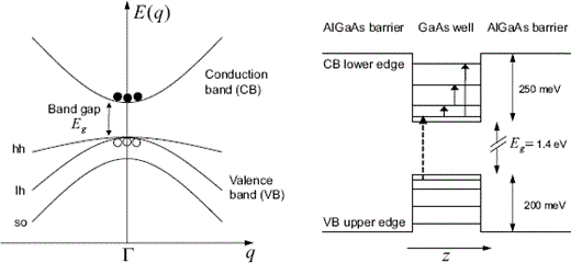
Figure K.2 shows a small portion of the electronic band structure of a so-called direct semiconductor (for example, GaAs) close to the zone center. In this region, the valence and conduction bands are parabolic, which means that they have energy dispersion relations similar to that of a free electron (ħ 2 q 2/2m), except that the cur-vatures suggest that their masses are different from the free-electron mass m. The effective electron mass (m*) and hole masses in a semiconductor are usually much smaller than the free-electron mass m. In the following, we focus on the conduction electrons.
Left: band structure of a direct semiconductor around the zone center (the Γ-point). The valence band consists of heavy holes (hh), light holes (lh), and split-off (so) states. Electrons tend to sink to the bottom of the conduction band; holes float on the top of the valence band. Right: electronic levels and optical transitions in a GaAs/AlGaAs quantum well. Interband transitions (dashed arrow) have energies of the order of the band gap Eg. Intersubband transitions (full arrows) have much lower energies, in the range of 10–10 meV.
Let us now apply the effective-mass approximation to describe electrons in a quantum well. The single-particle states are free-electron-like in the x–y plane, but experience finite-size quantization along the z direction. This suggests the following form:
where rǁ = (x, y) and qǁ = (q x, q y) are the in-plane position and wave vector, and A is the area. Notice that the band index n has been dropped, since we consider only conduction band states, and we have introduced the subband index j (defined below). The envelope functions φ jqǁ (z) follow from a one-dimensional Kohn–Sham equation:
where m*(z) accounts for the different effective masses in the well and barrier materials.1 Often one can ignore the z-dependence of m* and simply use the effective mass of the well material throughout. This is justified since the subband wave functions do not penetrate much into the barrier, and the effective masses of GaAs and Al0.3Ga 0.7As are not that different anyway. In that case we can write everything in effective-mass atomic units (see Appendix A), and eqn (K.2) simplifies to
i.e., the envelope functions are independent of qǁ, and the subband energy dispersions are parabolic:
The Kohn–Sham potential is given by υ s(z) = υ conf(z) + υ H(z) + υ xc(z). Here, υ conf is the bare confining potential of the quantum well, typically a square-well potential, but other shapes are also possible by gradually varying the material composition.2 The Hartree potential follows from integrating Poisson's equation:
For the xc potential, we use the LDA in its three-dimensional form.
The ground-state density n 0(z) is obtained as
The conduction band Fermi energy E F is determined via the given sheet density N s (typical values of N s are in the range 1010–1011 cm–2):
where N occ is the number of occupied subband levels, and we assume the φ j’s to be normalized to one. Figure K.3 shows a characteristic example of a narrow quantum well containing three bound subband levels, where only the lowest one is occupied.
![Subband envelope functions and energy dispersions [eqn (K.4)] for a quantum well. Here, only the lowest subband is occupied, as indicated by the conduction band Fermi level E F. Intersubband transitions may occur with zero and finite momentum transfer k∥.](https://oup.silverchair-cdn.com/oup/backfile/content_public/books/10143/parts/acprof-9780199563029-appendix-11/2/m_acprof_9780199563029_graphic_142.gif?Expires=1716640846&Signature=ZnI8PJJ-o5JBc5Njcp5mwPYsKLcvGicyd0GpzQliKCf9yAsnVYx2R4xMrr~lQJ6~5R2ge4B0lIbFa4uXjn5pvx6xvFD7hBhgA8H1-ghwQdsSiLSHK0opFLmLnPzbZNjiHsF-pTmJHL0LDnG5bY6Ocrhywqdx10h2eAWsf7xSDGChcGm9TRsAgmbjHufBPUUgObOuRA~xDaly~4pP4MHxjyVuXAxzf-WzW4-CaD4L4fZMmaOScJSIgk2mQ3Ibnip3xl1Mtv7kXP5Z8aaKgubMrG7uDWPXOAInep1MwK8f2ZzgP-nCqhy6-lmQ1ldE6tf1~XUzl8xhh72Gy8bi50gzGQ__&Key-Pair-Id=APKAIE5G5CRDK6RD3PGA)
Subband envelope functions and energy dispersions [eqn (K.4)] for a quantum well. Here, only the lowest subband is occupied, as indicated by the conduction band Fermi level E F. Intersubband transitions may occur with zero and finite momentum transfer k∥.
Equations (K.3)–(K.7) constitute the most elementary DFT approach to describing the self-consistent subband structure of quantum wells, and are in fact quite accurate for the widely studied GaAs/AlGaAs systems. There are, however, situations where one needs to do better than this, for example in the case of materials with a smaller band gap such as InAs/AlSb. A powerful method to calculate the electronic structure of semiconductors close to the band extrema is the so-called k·p approach, where one expands in terms of a basis of valence and conduction band states at the zone center, including some semiempirical parameters to get the correct band gap. We will not discuss any technical details here (see Davies, 1998; Harrison, 2005), but will merely point out two interesting consequences emerging from a more rigorous treatment:
The subband energy dispersions deviate from parabolicity, owing to an energydependence of the effective mass. The bands are also warped to some extent, although this effect is much stronger for the valence bands.
In the presence of spin-orbit coupling, spin is no longer a good quantum number.For systems without inversion symmetry, the quantum well subbands acquire aqǁ-dependent spin splitting.
K.2 Intersubband dynamics
Let us now consider intersubband excitations in a quantum well. Since our quantum wells are translationally invariant in the x–y plane, we write the TDDFT linear spindensity response equation (7.84) in a mixed representation:
The Kohn–Sham response function (7.86) becomes
The envelope functions φ j(z) follow from eqn (K.3), and with ω lj = ε l – ε j we have
The qǁ-integral in eqn (K.10) can be evaluated analytically for all kǁ (Eguiluz, 1985). The linearized effective potential is given by υ s1σ = υ 1σ + υ Hxc1σ, where
We choose the following external perturbation to excite intersubband excitations with a finite in-plane wave vector:
which couples to the charge (+) and the spin (–) channel via , respectively. Having solved the response equation (K.8) self-consistently, we obtain the absorption cross section as
The intersubband plasmons correspond to sharp peaks in σ(kǁ, ω), whereas the singleparticle continuum causes a broad, diffuse bump in the absorption spectrum.
Of particular interest is the case of zero momentum transfer (see Fig. K.3), corre-sponding to vertical intersubband transitions. We have
In this case, the external perturbation reduces to the usual dipole approximation for linearly polarized electromagnetic waves, , and the photoabsorption cross section becomes
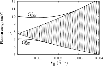
Figure K.4 shows the spectrum of excitations for a 40 nm GaAs/Al0.3Ga 0.7As square quantum well with N s = 1 × 1011 cm–2, where only the lowest subband is occupied in the ground state. The shaded area represents the region of incoherent particle-hole excitations (Landau damping), which arise from the poles of the Kohn–Sham response function where the denominator in eqn (K.10) vanishes. Comparison with Fig. K.3 shows that all vertical (k ǁ = 0) single-particle intersubband excitations have the same energy, ω = ε 2 – ε 1 ≡ ω 21. At finite k ǁ, single-particle excitations with different energies are possible, which accounts for the opening up of the Landau damping region.
Intersubband charge-and spin-plasmon dispersions for a 40 nm GaAs/AlGaAs quantum well, . The shaded region indicates Landau damping.
The plasmon excitations are separated from the Landau-damping region. We can use the small-matrix approximation of Section 7.6 to solve the response equation analytically. Keeping only those terms that contain the first and second subband in the Kohn–Sham response function, we have, for k ǁ = 0,
Defining
we get the intersubband plasmon frequencies
The Hartree contribution in S σσ′ is known as the depolarization shift, and the xc con-tribution is sometimes (somewhat misleadingly) called the excitonic shift. The Hartree part always induces an upshift in the plasmon frequency with respect to ω 21, and the xc part gives a smaller downshift. In ΩcISB, the positive shift dominates, but for the spin plasmon, the Hartree parts cancel out in eqn (K.18) and ΩISB is redshifted (see Fig. K.4). This is a remarkable result: the existence of the intersubband spin plasmon is purely a consequence of f xc,σσ′.
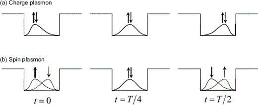
Figure K.5 shows how the intersubband plasmon excitations look like in real time. The charge plasmon is a simple collective sloshing motion of the density perpendicular to the quantum well plane, along the direction of confinement. The spin-up and spin-down densities move together in the charge plasmon, but they move in opposite directions in the spin plasmon. This is indicated by snapshots of the densities during the first half-cycle of the oscillations.
Real-time dynamics of charge and spin plasmons in a quantum well. In the charge plasmon, the spin-up and spin-down densities move in phase, and in the spin plasmon they move out of phase.
The peculiar form of the kinetic-energy operator used here ensures conservation of current at the interfaces (Davies, 1998).